Research progress of millimeter wave antenna integration technology

Abstract: As the technical support of 5G large-scale multiple input/multiple output (MIMO), millimeter wave antenna integration technology is a key technology to realize high-resolution data streams, mobile distributed computing and other application scenarios. Discussed the development status, key technologies and solutions of millimeter wave antenna integration technologies such as packaged antenna (AIP), antenna on chip (AoC), hybrid integration, etc., analyzed several typical integrated antenna technologies, analyzed the technological development context, and summarized 5G The development trend of millimeter wave integrated antenna integration technology.

For example: for vital signs monitoring and gesture recognition, IMEC has developed a 140GHz FMCW radar transceiver with an on-chip antenna. The radar has a working range of 0.15m to 10m, a resolution of 11mm, a radio frequency bandwidth of 13GHz, and a center frequency of 145GHz. The transceiver IC is manufactured using 28nm module CMOS technology, which can realize a low-cost solution.
Introduction

The millimeter wave semiconductor is the basic device of the fifth generation mobile communication technology (5G), and the technology of using millimeter wave frequency for directional communication is one of the key technologies of the expected 5G configuration. The frequency range of millimeter waves is 30 to 300 GHz. The bands currently studied include 28 GHz band, 38 GHz band, 60 GHz band and E band (71-76 GHz, 81-86 GHz). 5G technology shifts the communication frequency band to millimeter wave frequencies much higher than the fourth-generation mobile communication technology (4G). Compared with 4G, the spectrum bandwidth of 5G will be increased by 10 to 20 times, the maximum data transmission rate can be increased by 20 times, and the size of antenna array and base station equipment is smaller and the cost is lower. Among the millimeter wave frequency bands, the 28 GHz frequency band and the 60 GHz frequency band are the two most promising frequency bands for 5G applications.
As a passive component for sending and receiving RF signals, the antenna determines communication indicators such as communication quality, signal power, signal bandwidth, and connection speed, and is the core of the communication system. How to increase spectrum data throughput is a major challenge from 4G to 5G. The key technology of 5G is the massive multi-input, multi-output (MIMO) integrated millimeter wave antenna technology. Each MIMO channel has its own signal path from the receiving antenna, the transmitting antenna to the microprocessor. The function of the receiving channel is to realize the down-conversion from the RF signal received by the antenna to the input sampling baseband frequency, and functions such as analog-to-digital signal conversion. The function of the transmit channel is to convert the up-converted digital signal into an analog RF signal. Downsizing is an important challenge for 5G antennas. The smallest base station antenna size will shrink to the size of a credit card, which will increase the integration, low power consumption and connectivity requirements of millimeter wave antennas and circuits. Improving power density is another important challenge for 5G antennas.
Multi-antenna system integration is one of the key technologies to deal with the challenges of 5G system MIMO, downsizing, and increasing power density. Since SiGe and CMOS RF integrated circuits have reached high fT, fmax and high integration density, CMOS, SOI and SiGe processes can be used to design large-scale fully integrated silicon millimeter wave phased array circuits. Based on the full RF structure, 8-32 yuan transmit (Tx), receive (Rx) or receive/transmit (T/R) modes have been successfully used in the 45-110 GHz frequency band. The silicon integration solution can integrate multiple components on the same chip. Compared with Group III-V semiconductor technologies such as GaAs and InP, silicon-based technologies have higher integration and lower costs. Silicon phased array chips are widely used in the millimeter wave field. The challenge faced by this technology is that the RF power amplifier, low-noise receiver amplifier, A/D converter or D/A converter on the signal chain unit all require great efficiency improvements.
Both wireless communication and sensor systems can improve performance through the use of RF systems to improve integration and the use of new packaging technologies. There are currently three schemes for realizing front-end circuits and integrated antennas. The first is the antenna packaging (AIP) technology, where the antenna is manufactured using IC packaging technology. The second is the antenna on chip (AoC) technology, where the antenna is directly fabricated on a silicon substrate. The third is a hybrid technology of AiP and AoC. The antenna feed point is made on the chip and the radiating element is realized off-chip. In AiP technology, the interconnection of the chip and the antenna should achieve effective signal transmission efficiency within a certain frequency range. The main packaging processes include wire bonding and flip chip technology. However, the loss of the device at high frequency is large, and the cost will increase.

1 Structure of phased array receiver

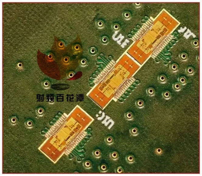
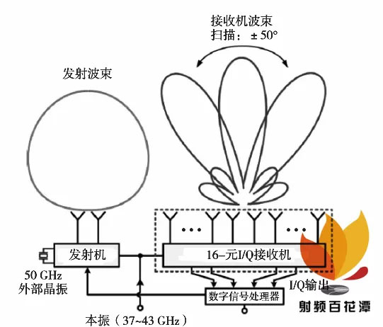
The application range of silicon millimeter wave phased array technology in 5G communications continues to expand. Many companies use SiGe and CMOS processes to make ICs, and their operating frequencies have reached 60-100 GHz. For example, Toyota Research Institute in North America has developed a SiGe single-chip automotive phased array receiver with RF beamforming capability [1], as shown in Figure 1.
The automotive phased array receiver is packaged with low-cost bond wire technology and connected to a 16-element linear microstrip array. The antenna has a directivity of 29.3 dB at a frequency of 77 to 81 GHz, a gain of 28 dB, and can scan to ±50° in the azimuth plane per step (1°). In this chip, the spacing of the planar phased array antenna array is only 0.5λ (λ=3.75 mm, frequency below 80 GHz). This parameter is especially important for millimeter wave circuits with a small usable area. This kind of phase array needs to integrate as many circuits as possible on SiGe or CMOS chips, including not only phase shifters and VGAs, but also all transmit/receive circuits, power synthesis networks, digital and SPI control, and bias circuits. In some cases, a complete up/down converter is also included.

Figure 1 Millimeter wave automotive phased array receiver
2 Antenna integration technologyCurrently, 60 GHz packaged antennas and on-chip antennas are designed using commercial electromagnetic simulation software. For hybrid solutions, modeling methods that complement standard IC design tools have been developed to achieve coordinated integration of wire bonding and IC. AiP technology requires a broadband low-loss interconnection design between IC and antenna to ensure overall performance. AoC technology requires advanced post-processing steps or packaging processes to reduce severe dielectric loss. Hybrid antenna integration technology combines the advantages of AiP and AoC to achieve high radiation efficiency without the need for low-loss interconnection design of chips and packages. However, the design flexibility of this scheme is not high, and the radiation zero point appears in the wide side direction, which prevents its application in some occasions.

2. 1 AiP technology
2. 1. 1 Structure

AiP technology is a key technology for integrating one-element or multiple-element antennas into the RF package, and its typical solution is to use integrated circuit packaging technology. In the silicon millimeter wave transceiver, the antenna array is integrated in the package to help provide sufficient signal gain and minimize the size. This process is the key technology for the large-scale application of millimeter-wave RF integrated solutions. For example, the size of a 30 GHz antenna element is on the order of millimeters, and a new type of antenna array integration technology needs to be adopted in a single package. The tiny phased array antenna with beam steering function is the key component of millimeter wave radio [2]. In order to integrate the antenna array in the transceiver package, it is necessary to consider the chip assembly scheme, array elements and feeder network, chip and package interconnection, packaging materials, etc. If the transceiver adopts a multi-layer package, it is necessary to adopt advanced interconnection technology between the chip and the antenna to meet the minimum requirement of antenna feed insertion loss. The chip can be placed on the front of the package or on the bottom of the package.
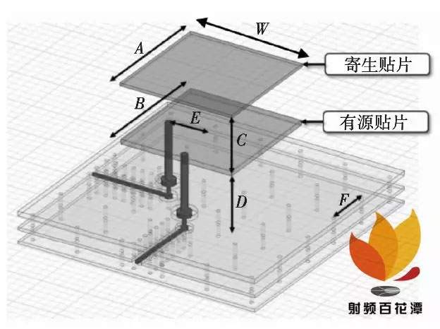
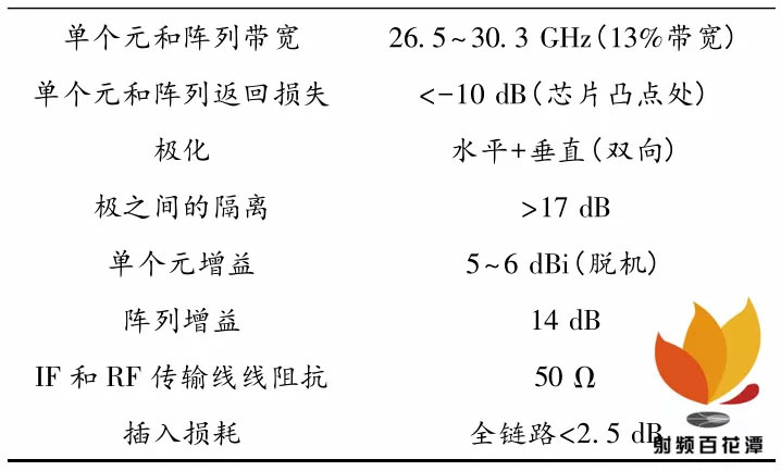
The solution of placing the chip on the bottom of the package has the least impact on chip reception and transmission. A phased array millimeter wave antenna in an organic chip package that can be used for 5G wireless communication is shown in Figure 2. In order to improve the antenna bandwidth, gain and radiation efficiency, a parasitic plane structure is placed on a thick cover plate to form a dual patch antenna stack. In order to achieve the goal of optimizing RF design and manufacturing, the parameters of package laminates and low dielectric constant materials have been optimized, as shown in Table 1.

Figure 2 Phased array millimeter wave antenna in organic chip package
Table 1 Antenna array design requirements
2. 1. 2 Design and manufacturing

In AiP design, in addition to beamforming, signal amplification and phased array IC with frequency conversion functions, antennas with polarization characteristics are also key components of the antenna array. In the earliest silicon-based millimeter-wave IC design and development stage, the antenna design uses technologies that are compatible with silicon-based millimeter-wave ICs in terms of substrate, shape and cost [3]. At present, there are millimeter wave antennas on silicon substrates with multiple frequencies. However, due to the large area and limited emission efficiency, antennas above 100 GHz have research value. In 60 GHz frequency, in liquid crystal polymer (LCP), organic high-density interconnect substrate, glass substrate, high/low temperature co-fired ceramic substrate, silicon substrate and molding material-based wafer-level substrate The silicon phased array antenna array fabricated on has been reported. It is usually necessary to optimize the gain, bandwidth and radiation pattern of the AiP array. At the same time, factors such as substrate material, array size (that is, the number of components and patches), interconnection flexibility (such as connecting power and control signals), compatibility of thermal and mechanical properties, IC assembly and board integration need to be considered .
A new antenna and IC/carrier structure is shown in Figure 3 [4]. The antenna structure is fabricated on a dielectric substrate with a thickness of T through a PCB board, and is suspended upside down, flipped over the IC/carrier. The ground of the IC package base is also used as the mirror ground of the antenna, and the distance between the antenna and the ground is H. In this structure, there is a very low dielectric constant between the antenna and the floor, and a layer of cover material with a higher dielectric constant is placed on the antenna structure. On the premise of maintaining high antenna efficiency, this stacked structure has a higher bandwidth than standard PCB antenna structures. A pad with solder balls can be placed on the other end of the antenna cover as a support.

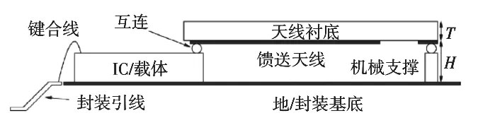
Figure 3 Antenna and IC/carrier structure

In AiP design, integrated circuit packaging technology is usually used for packaging, and the antenna needs to be physically connected to the on-chip circuit. The low-temperature co-fired ceramic (LTCC) process can realize any number of layers of mounting structure, with the flexibility of cross-layer vias, formation of open or closed cavities between layers (IC can be integrated here). The millimeter wave antenna packaged by this process has attracted more and more attention [5]. Some solutions use traditional bonding wire, flip chip and C4 soldering processes. For example, a 60 GHz silicon phased array chip package requires a multi-layer millimeter wave substrate with a low-loss distribution network between the chip and the antenna. It must be a multi-layer low-loss Teflon-based or LTCC-based, which is expensive. Therefore, the typical silicon phased array AiP can reach a frequency of 30 to 60 GHz [6], and it is more difficult to reach 80 GHz.
Compared with the LTCC package solution, the printed circuit board (PCB) package solution can reduce costs. There are packaging schemes that use low-cost high-frequency circuit materials such as PCBs to make multilayer mounting structures, such as the RO3000 series and RO4000 series [7-8]. There is also a low-cost solution using liquid crystal polymer as the substrate. However, due to the use of blind vias or buried vias, the number of layers increases, which will increase the mechanical manufacturing cost of PCB technology. In addition, it is more difficult for PCB technology to achieve high-density in extremely high frequency bands, which will seriously affect system performance and result in reduced efficiency. Therefore, the LTCC process is the choice of most multi-layer structure arrays, and the performance of antennas using this process scheme is improved.

2. 2 AoC technology
2. 2. 1 On-chip antennaThe on-chip antenna is an antenna integrated and manufactured using on-chip metallization and wiring technology. The method of directly integrating and combining antennas on the chip is one of the least researched areas of terahertz communication devices. Under current technical conditions, due to the substrate absorption and conduction current, eliminating all the connections between the RF circuit and the antenna will greatly reduce the design cost and make the design more flexible. Conventional wisdom believes that because there is no compensation structure for dielectric lenses, the on-chip antenna is not the best structure for consumer low-power devices. Although the efficiency of a typical on-chip antenna can only reach 10%, if a sub-millimeter antenna can be designed and manufactured on the chip (using a frequency-selective surface [9] or Yagi’s highly directional antenna [10]), it will bring The advantages of a substantial reduction in cost and a substantial increase in design flexibility will exceed the advantages of using more efficient, but expensive and complex off-chip antennas, thereby increasing the possibility of applications.
As the carrier frequency and bandwidth move to Asia-Pacific Hertz, the high bandwidth and high carrier frequency make the metal leads become unstable, and the on-chip antenna is considered to be one of the methods to replace the metal interconnection of the chips on the printed board. In addition to on-chip antennas, on-chip waveguides and through-silicon vias (TSV) waveguides are also promising technologies for replacing metal wiring in large bandwidth applications in the Asia-Pacific Hertz band. The successful implementation of on-chip antennas will benefit many applications such as highly integrated transceivers, 60 GHz space power supply combinations and higher frequency millimeter wave systems. There have been many reports on on-chip antennas with multiple frequencies ranging from 0.9 GHz [11] to 77 GHz [12]. The German Institute of High-Performance Microelectronics (IHP) designed and fabricated a 130 GHz on-chip antenna using standard SiGe BiCMOS technology, with a peak gain of 8.4 dBi.

2. 2. 2 CMOS on-chip antennaCMOS technology is an important development path for RF IC. With the characteristic frequency (fT) of CMOS tube approaching 400 GHz [14], CMOS technology has been further applied in millimeter wave ICs. Literature [15] proposed a new method of integrating artificial magnetic conductors and broadband narrow slot antennas on CMOS chips, using standard CMOS technology to achieve a gain of 2 dBi at 60 GHz and an impedance bandwidth greater than 126%. The literature [16] used a 0.18 μm CMOS process to produce a 60 GHz circularly polarized loop antenna with a simulated and measured axial ratio (AR<3) bandwidth and gain covering 57~67 GHz. Up to 4. 4 dBi. Literature [17] used Si CMOS technology to make devices with an impedance bandwidth of 25 GHz (45~70 GHz), and fabricated a 60 GHz wideband monopole antenna, which achieved-4. 96 dB at 60 GHz. Gain. Literature [18] proposed a high-gain (8 dBi maximum gain) and high-efficiency (96.7% peak antenna efficiency) on-chip antenna, which was fabricated using CMOS 0. 18 μm process, and the antenna’s -10 dB bandwidth was 4 GHz . Literature [19] used a 0.18 μm CMOS process to produce a CPW-fed loop monopole antenna with a bandwidth of 60 GHz.
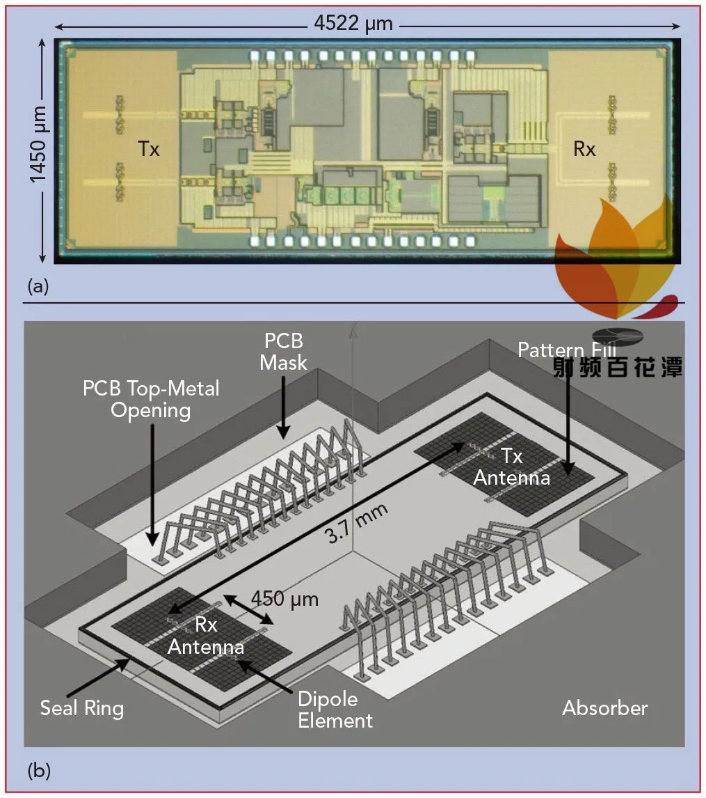
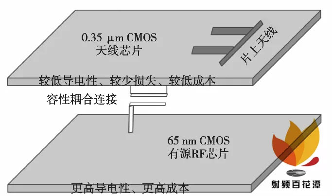
Generally, on-chip antennas fabricated on doped silicon substrates are only about 10% inefficient. However, if a higher cost package antenna is used, higher efficiency can be achieved than on-chip antennas. Capacitive coupling and other advanced connection technologies can be used to connect the antenna chip made on a mature, low-cost, and less-doped substrate with an active 60 GHz millimeter-wave RF chip, so as to achieve a better device than the standard bonding process Much higher operating frequency range. The antenna can be made with a low-cost process (such as 0.18 or 0.35 μm) and a low-doped substrate, and then connected to active components such as a 60 GHz power amplifier through capacitive coupling. Using more advanced technology [20]. A millimeter-wave integrated antenna that connects the antenna chip and the active 60 GHz RF chip through capacitive coupling is shown in Figure 4. The antenna not only has the low conductivity and low loss substrate due to the low doping concentration and high resistivity of the old process, but also has higher efficiency. When making antenna arrays, low-speed active switches (such as diodes) can be integrated on the chip, and phase-divided passive feeders are used to perform component tuning, phase shifting and wave speed control.

Figure 4 A millimeter-wave integrated antenna that connects the antenna chip and the active 60 GHz RF chip through capacitive coupling
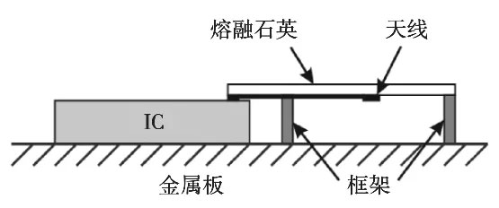
2. 3 Hybrid integrated millimeter wave antennaThe hybrid integrated millimeter wave antenna uses a dedicated process to integrate the antenna and the front-end IC in the same package. This production technology is an alternative to pure AiP and AoC. The schematic diagram of the hybrid integrated antenna is shown in Figure 5 [21]. One half of the dipole antenna on the fused silica substrate is mounted on the chip, and the other half is mounted under the chip. The antenna of this structure can be directly connected to on-chip electronic devices. In the full frequency band of 60 GHz, when the gain is 6-8 dBi, the maximum radiation efficiency of the chip can reach 90%.

Figure 5 Conceptual schematic diagram of hybrid integrated antenna
3 Progress in millimeter wave antenna integration technology
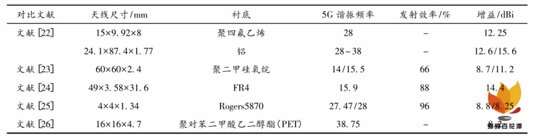
3. 1 The development of academiaTo achieve the goal of comprehensive interconnection between the Internet of Things (IoT) and 5G, it is necessary to develop antennas in different millimeter wave frequency bands and achieve commercial mass production. Table 2 summarizes the millimeter wave antennas and their performance comparisons in recent literature for wide-area IoT and 5G wireless communications. It can be seen that there are still few practical solutions, and most solutions still need to solve the problems of complex structure, reduced gain, low efficiency and high power consumption.
60 GHz millimeter wave band devices will be applied to 5G and mass production. The development trend of system-on-chip or on-chip front-end miniaturization system integration requires that the cost, size, and power consumption of AoC devices and AiP devices must be developed in a smaller direction without sacrificing radiation efficiency, bandwidth, and gain. The use of silicon IC technology provides maximum integration, low cost, and low power consumption, indicating that GaAs and other III-V compound processes are not necessarily the best choice, especially when packaging, integration, and interconnection issues are considered.

Table 2 5G millimeter wave antenna and its performance comparison in recent literatureThe antenna element is usually made off-chip, but it can also be completely integrated on a single chip. Due to the high dielectric constant and low resistivity of the silicon substrate, the gain of the on-chip integrated antenna is very small and the radiation efficiency is very low. The performance can be improved by increasing the resistivity of the substrate. For example, when making a high-performance and low-cost SoC, the antenna and IC are integrated into high-resistivity silicon on insulating layer (HR SOI). In the AiP solution, in order to solve the problem of excessive insertion loss of the planar feeding device of the antenna array on the silicon substrate at millimeter wave frequencies, a hybrid integrated innovative technology that integrates the antenna on an additional substrate can be used to make full use of the packaging and A coupling possibility in a limited space. This scheme shows high design flexibility.
IBM has developed the RFIC and AiP series in the past 14 years: performance-driven phased arrays with beamforming and beam scanning capabilities for imaging and communication applications (such as 60 GHz, 94 GHz and 28 GHz phased arrays), supporting portability The device’s V-band, W-band and Ka-band millimeter wave modules (such as 60 GHz single element, switched beam module) [27].
Literature [28] proposed a linearly polarized 6 GHz antenna array constructed on a multilayer LTCC substrate. These arrays use 4×4 microstrip patch radiating elements, respectively fed by a quarter-wavelength matched T-connector network and a Wilkinson power divider network. The measurement results show that the array fed by the former performs better than the array fed by the latter. For arrays with and without embedded cavities, the measured impedance bandwidths are 9.5% and 5.8%, and the maximum gains are 18.2 dBi and 15.7 dBi, respectively.
Literature [29] reported a linearly polarized 60 GHz antenna array constructed on a fused silica substrate. The array uses 2×4 microstrip patch radiating elements fed by a feed network, which uses coplanar strips and coplanar strip waveguides. The array enhanced by the metal cavity achieves a measurement impedance bandwidth greater than 9 GHz and a maximum gain of about 15 dBi.
Literature [30] proposed an antenna array with 2×2 microstrip patch radiating elements using LTCC technology to produce a 60 GHz transmitter module with linear polarization.
Literature [31] used 1×8 and 2×5 microstrip patch radiating elements to fabricate two active linearly polarized 60 GHz antenna arrays.
Literature [32] proposed a linearly polarized 60 GHz antenna array with slot radiating elements fed by a wave-back waveguide network.
Literature [33] proposed a circularly polarized 60 GHz antenna array, which achieved a wide bandwidth by finely designing the original antenna elements, laminated waveguides, and adjusting the circular polarization axis ratio.
Literature [34] proposed a circularly polarized 60 GHz antenna array fabricated on an LCP substrate. The array uses a new slot radiating element and a novel open-cavity reflector. The measurement results show that the peak gain of the 2×4 radiating element array is 15. 6 dBic.

3.2 Development trend of commercialization

According to Gartner’s forecast, by 2021, 9% of smartphones in the market will support 5G networks. 5G uses beamforming technology and must use a multi-antenna array system (Massive MIMO). This will lead to an order of magnitude increase in antennas, and promote the development of antennas in a highly integrated and complex direction, with continuous upgrading of process technology and continuous application of new materials. For example, the new material liquid crystal polymer (LCP) material has the advantages of low loss, high flexibility, high sealing, etc., which is very suitable for making microwave and millimeter wave devices. The millimeter wave antenna solution introduced by Apple includes antennas made of LCP materials, which is an important direction for the large-scale commercialization of 5G antennas [35]. Qualcomm’s QTM052 millimeter wave antenna module series supports compact package size and is suitable for mobile terminal integration. Terminals equipped with QTM052 millimeter-wave antenna modules will be launched on the market in the first half of 2019, showing the development trend of integrating antennas and RF front-end components in 5G. STMicroelectronics, STATS ChipPAC and Infineon Technologies have jointly developed the next generation eWLB semiconductor product packaging technology based on Infineon’s first-generation embedded wafer level ball grid array (eWLB) technology. A four-channel transceiver made of an integrated antenna with an 8 mm×8 mm package has been developed. The antenna adopts the metal structure in the RDL layer and is integrated in the package, providing a solution for radar system packaging applied in the millimeter wave field such as 5G [36]. Recently, SMIC released the world’s first ultra-wideband dual-polarized 5G millimeter wave antenna chip wafer-level integrated package made on the SmartAiPTM process platform. It has the characteristics of high integration, good heat dissipation, and simple process. Realize 24-43 GHz ultra-wideband signal transmission and reception, and achieve an ultra-high antenna gain of 12. 5 dB.

4 Conclusion

For a long time in the future, the 5G architecture will continue to evolve in the network, wireless access, and physical layers. It is necessary to have a variety of innovative product combinations in RF/millimeter wave integrated circuits, millimeter wave antenna array technology, etc., to promote 5G Radio and industrialization development. For example, the number of power amplifiers, antennas, filters, and matching circuits in 5G can be as high as 64 or more. The improvement in efficiency and integration of these components is very important to the overall energy efficiency and performance of the radio. A highly integrated MIMO radio with a large number of antennas and a frequency of 27 GHz and above is the key technology of the 5G system. The above three integrated solutions can be used for millimeter wave antenna design. Taking the 60 GHz frequency band as an example, the radiation efficiency and gain indicators of AoC devices lag behind AiP devices and hybrid solutions. AiP devices and hybrid devices achieve the best radiation efficiency, so it can be considered that AiP technology is more appropriate than AoC technology. AiP technology has the advantages of design flexibility and printed antenna structure, but for complex multilayer packaging structures, it may not have the conditions to compete with AoC technology and hybrid solutions at the same cost. In addition, the chip-to-chip interconnection of the AiP solution will cause heat loss, delay, and increased design effort. The hybrid solution seems to be the best solution. However, when the frequency exceeds 60 GHz, the typical hybrid technology and AiP are not mature solutions. The AoC program will be more complete and has been tested in the THz band. It is expected that the AoC program has more room for development at high frequencies.
A fundamental solution for antenna integration is to integrate everything required for a phased array on a chip, which is the advantage of the silicon-based millimeter wave antenna system. Not only integrated electronic devices, but also integrated high-efficiency antennas leading to wafer-level implementation. The wafer-level phased array can be placed on a low-cost printed circuit board with input/output data signals up to Gbit/s and arranged with control devices and power devices. The entire millimeter wave function is integrated on the same chip. This wafer-scale implementation is a completely self-contained solution. (References omitted)

Author: Wang Wenjie, Qiu Sheng, Wang Jianan, Lai Van

Another breakthrough in mobile phone millimeter wave antenna design: innovative mobile phone antenna design based on AiAiP, compatible with full screen, 60-GHz millimeter wave, and LTE antenna!

In addition to the well-known 5G millimeter wave application of millimeter wave technology on mobile phones, another potential emerging application is 60-GHz millimeter wave motion (such as gestures or head movements) recognition radar. The display is an extremely important and dominant feature of mobile phones. With the full-screen trend that began in 2017, for today’s mainstream mobile phones, the design of large screens or high screen-to-body ratios has long become the standard basic Configuration. However, for most of the user’s mobile phone wireless control movements, especially gestures or head movements, the detection direction is often toward the front of the display screen, which implies that the radiation pattern of the radar antenna should be out of the screen and face the user. Direction. The current mainstream design is to open an antenna window without metal obstruction (such as notch notch) on the display screen, and place a 60-GHz millimeter wave AiP (antenna-in-package) solution under this window (or directly adopt a non-high The screen-to-body ratio is designed to be able to install a 60-GHz millimeter-wave AiP module in the non-screen area); in this way, the radar beam can better radiate out of the screen and face the user to help the user’s wireless control experience . However, this design often affects and even hinders the high-screen-to-body ratio or full-screen design of the mobile phone, and the look and feel of the display screen is often the top priority of the mobile phone as mentioned above. Therefore, how to be compatible with full-screen and 60-GHz millimeter wave motion recognition radar on mobile phones has become a new hot topic in mobile phone antenna research and design.
Recently, a research article submitted by the antenna pre-research team of vivo mobile communication company last year based on AiAiP [1]–[3] mobile phone millimeter wave antenna innovative design to be compatible with mobile phone full screen and 60-GHz millimeter wave antenna [4] Published online at this year’s EuCAP (European Antenna and Propagation Conference), this innovative design will not only contribute to the expansion of new ideas for the compatible design of future mobile phone full screens, 60-GHz millimeter wave antennas and LTE antennas, but also this design. It incorporates the coverage of the millimeter wave antenna by the screen glass of the mobile phone and glass adhesive, so it has more practical design guidance function.

The author of the article stated: “The main framework and ideas of this research originated in the second half of 2018. The relevant patent application was filed before the submission of the article in 2019, and this design concept inherits the AiA proposed by the antenna pre-research team. [5]–[6] and AiAiP [1]–[3] thinking, that is, transforming the metal frame that was unfavorable or restrictive to the antenna design into an antenna carrier that is beneficial and helpful to the antenna design, so as to break through the original It is compatible with the full screen design, and achieves the purpose of effective radiation and more competitive products. Because the radiation direction of the millimeter wave antenna based on the metal frame design needs to go out of the screen and face the user, but it is limited The thickness of the metal frame and the limited stacking space in the machine, the general form of antenna design scheme [7]–[10] is often difficult to meet the requirements of product and radiation at the same time, so the scheme here is to design embedded on the metal frame. The H-plane sectoral horn antenna uses a narrow metal frame as the boundary metal of the horn antenna (because the H-plane sectoral horn antenna is parallel to (not orthogonal to) the metal frame) Long-side opening, so there is no need to increase the thickness of the metal frame, that is, it does not affect the active area of ​​the full screen (that is, the proportion of the AA area) and can obtain the desired output screen and the radiation direction toward the user Figure, and this 60-GHz millimeter wave antenna is further embedded and integrated with the metal frame LTE antenna, so the two types of antennas can share the metal structure to achieve a more compact design that overcomes metal shielding; in addition, if the whole If the machine conditions permit, this design can also be placed in multiple layouts to achieve a better wireless control experience for users. I would like to give some thoughts to teachers, scholars and experts, and friends to advance and give guidance to Kuang Axe.”

The following are mainly excerpts selected from the aforementioned published articles (except for detailed dimensions and parameters) to share relevant design ideas. This design and simulation is based on the electromagnetic simulation software Dassault System Simulia CST 2018, and as shown in Figure 1 below, the appearance of this mobile phone has a metal frame and both front and back sides are covered with 100% glass (the front and back sides are the same) and are Typical actual size model. In the picture, the yellow part is metal, the blue part is the screen glass, and the brown part is the dielectric encapsulation. Figure 2 is a front view of the inside of the mobile phone with the screen glass removed. Figure 2 shows that four 60-GHz millimeter wave antennas (one of which is a transmitting antenna and three are receiving antennas) are embedded and integrated in metal In the frame, and this metal frame also serves as an LTE low and high frequency antenna, the visible area of ​​the screen (ie AA area) accounts for more than 91.7% of the entire front of the phone. Figure 3 is an internal view with the back cover glass removed. There are two T-shaped slits (narrow outside and wide inside) on the top and bottom metal frames to facilitate the design of the LTE antenna. The dimensions in Figures 1–3 are all millimeters (mm).

Figure 4 shows the oblique rear view layout of a single H-plane sectoral horn antenna, which is embedded in the semi-transparent middle metal frame in the figure (this metal frame is also an LTE low and high frequency antenna) , And the metal frames at the left and right ends can be used as LTE intermediate frequency and non-cellular antennas (such as GNSS or WiFi antennas). And Figure 5 is a perspective and enlarged view of this embedded H-face sector horn antenna. The gray horn antenna is filled with dielectric material, and the pink color is the adhesive tape along the metal frame and the glass. Figure 6 Shows the feeding pin of the horn antenna and its position. In addition, due to the self-shielding effect of the boundary metal of the horn antenna, the designed antenna is less sensitive to the overall system stacking and layout inside the metal frame, so it can have a more stable antenna performance, which can increase the system stacking and layout design. flexibility.

Figure 7 is a stacking diagram of the y-z plane based on the centerline of the horn antenna in the x-direction of Figure 4. It can be seen that this design takes into account the related practical factors of multiple mobile phone stacking in the environment near the millimeter wave antenna, such as screen glass, glass adhesive, The display body, the main board, and the glue filling in the T-shaped slit and the system. And based on the AiAiP design, as the low and high frequency LTE antenna, the inside of the metal frame also integrates the package from AiP et al. [11]–[15] as the feeding part to reduce the feeding part of the millimeter wave. The radiating part (radiating part) is based on AiA’s integrated embedded design; therefore, AiAiP = AiA (radiating part) + AiP package (feeding part). Figure 8 shows the LTE antenna design. Because the full screen squeezes the keep-out area of ​​the antenna, in order to achieve better antenna performance, this design uses an antenna carrier, which combines part of the LTE antenna. Lift up off the ground [16].

Figure 9 is a perspective view of the layout of four equally spaced and identical embedded horn antennas based on the single horn antenna of Figures 4-6 as the building block. P1’–P4′ correspond to the four horn antennas respectively Feeding port, Figure 10 shows the internal side view of the carrier board with packaged IC (such as RFIC and PMIC) and LTE antenna bracket, while P1–P4 on the IC carrier board (at this viewing angle, the position of P4 is blocked by the LTE antenna bracket ) Respectively correspond to 4 radio frequency ports (from the traces fanned out by 4 RFICs). These 4 radio frequency ports are connected to the feed ports P1’–P4′ of the 4 horn antennas on the aforementioned metal frame. Transmission of radio frequency energy. And Figure 11 is the inside side view with the shield and the connector (the LTE antenna bracket is hidden at this time for easy viewing). The exploded view of the overall mockup is shown in Figure 12.

Figure 13 is the simulation |Snn| performance comparison diagram of the two scenes of the single horn antenna of Figure 4 with and without glass and glass glue. It can be seen that glass and glass glue have a significant impact on the reflection performance of the antenna port. Of course, the real mobile phone design is a scene with glass and glass glue. For real scenes (with glass and glue), the bandwidth (|Snn| ≤–6 dB) is 56.84 GHz–65.18 GHz, so it can cover the commonly used 60-GHz motion recognition frequency band (57.0 GHz–64.0 GHz) . Figure 14 is the performance comparison diagram of the total efficiency of the simulated antenna and the simulated peak real gain (realized gain) of the single horn antenna in Figure 4 with and without glass and glass glue. For the real scene (that is, with glass and glass glue) In terms of viscose), the antenna efficiency in the entire band is higher than –2.90 dB, and the highest antenna efficiency value is –1.59 dB; the peak actual gain in the band is higher than 3.0 dBi, and the highest peak actual gain value is 5.61 dB.

Figure 15 shows the single horn antenna (hiding half of the horn antenna structure) in Figure 4 when there is glass and glass glue at φ = 90° at the three frequency points of 57.0 GHz, 60.0 GHz, and 64.0 GHz (low and medium) , High-frequency point) electric field distribution diagram, it can be seen that as the frequency increases, the reverse behavior of the electric field increases. Figure 16 shows the single horn antenna in Figure 4 at 57.0 GHz, 60.0 GHz, and 64.0 GHz in two scenes with and without glass and glass glue. The three frequency points of φ = 90° and θ = 90° are 2D. Parallel polarization (co-pol.) and cross polarization (x-pol.) simulated actual gain patterns (realized gain patterns). Figure 17 shows a single horn antenna with glass and adhesive coverage and Figure 18 shows a single horn antenna without glass and adhesive coverage. Simulated 3D actual gain radiation at the same three frequencies and the same scale. Directional map. Figure 16-18 shows that in the scene with glass and glass glue, the radiation pattern becomes more dispersed as the frequency increases; but in the scene without glass and glass glue, the shape trend of the radiation pattern is not Disperse as the frequency increases, so the coverage of glass and glass adhesive has a significant impact on the performance of the antenna.

Figure 19 is the simulation |Snn| performance comparison diagram of the four horn antennas in Figure 9 (in the actual scene, with glass and glass glue) and the single horn antenna in Figure 4. The reflection performance of the five antenna ports can be seen It is basically the same, and the bandwidth of |Snn| ≤-6 dB is 56.86 GHz-65.16 GHz, so it can cover the required 60-GHz frequency band. Figure 20 shows the isolation between the four horn antennas, and the worst in-band isolation is higher than 27.57 dB. Fig. 21 and Fig. 22 are simulation comparison diagrams of the antenna efficiency and peak actual gain of a 4-antenna horn antenna and a single horn antenna in a real scene (that is, covered with glass and glue). The antenna efficiency of the four horn antennas in the entire band is higher than –3.08 dB, and the highest antenna efficiency value is –1.59 dB; the peak actual gain in the band is higher than 3.29 dBi, and the highest peak actual gain value is 5.67 dBi.

Figure 23 below shows the actual gain pattern of the 2D parallel polarization and cross polarization simulation of the above four horn antennas at 57.0 GHz, 60.0 GHz, and 64.0 GHz on the two tangent planes of φ = 90° and θ = 90° . It can be seen from the figure that the radiation behavior of antenna #1 to antenna #3 is very similar, but the radiation behavior of antenna #4 is different from that of antenna #1–#3, mainly because antenna #4 is close to the aforementioned LTE antenna. Feeding structure, so the boundary conditions of antenna #4 are different from the other 3 antennas, but the radiation behavior within the 3-dB beam width of the main lobe is still close to the 4 antennas. Figure 24 shows the simulated 3D actual gain radiation pattern of antenna #1 to antenna #4 at 57.0 GHz, 60.0 GHz, and 64.0 GHz for a more intuitive understanding.

Figure 25 shows the simulated antenna efficiency and peak actual gain when antenna #1–antenna #3, the three antennas with similar performance, form a receiving linear antenna array while performing constant amplitude and phase feed at the same time. The antenna efficiency is higher than –2.99 dB, and the highest antenna efficiency value is –1.58 dB; the peak actual gain in the band is higher than 7.10 dBi, and the highest peak actual gain value is 10.27 dBi. Figure 26 shows the actual gain pattern of the linear array at 57.0 GHz, 60.0 GHz, and 64.0 GHz on the φ = 90° and θ = 90° two-section planes; Figure 27 shows the array at 57.0 GHz. , 60.0 GHz, and 64.0 GHz simulation 3D actual gain pattern.

Figure 28 shows the |Snn| and total antenna efficiency of LTE low and high frequency antennas. When |Snn| ≤ –6dB, the coverage bandwidth is 877 MHz–962 MHz and 2273 MHz–2753 MHz, so the LTE antenna can cover LTE Band 8 ( 880 MHz–960 MHz), Band 40 (2300 MHz–2400 MHz), and Band 41 (2496 MHz–2690 MHz), if you want to perform different low frequency bands (such as: LTE Band 17, Band 20, or Band 5, etc.) Overlay, tunable devices can be added. In the current LTE low-frequency (Band 8) and high-frequency (Band 40 and Band 41) bands, the lowest antenna efficiency is –3.83 dB and –1.73 dB, respectively, so it can perform wireless communication well. In addition, the isolation between the 4 millimeter wave horn antennas and the LTE antenna is higher than 24.86 dB.

Finally, in the conclusion part of this article forward-looking: “This design can be further integrated with the previously published 5G (fifth generation mobile communications) millimeter wave AiA [5] or AiAiP [2] solution, that is, the LTE antenna , 5G millimeter wave antenna array, and 60-GHz millimeter wave antenna are integrated in a three-in-one antenna design to be compatible with the product features of mobile phone metal frame and full screen and achieve a good user wireless communication and control interactive experience To achieve a more compact and competitive product design.”

references:

[1] H.-C. Huang, “Overview of 5G mm-Wave Antenna Design Solutions in Cellular Phones: AiP, AiA, and AiAiP,” IEEE Antenn

The State Council issued “Several Policies to Promote the High-quality Development of the Integrated Circuit Industry and Software Industry in the New Era”

A few days ago, the State Council issued the “Several Policies to Promote the High-Quality Development of the Integrated Circuit Industry and Software Industry in the New Era” (hereinafter referred to as “Several Policies”).

The “Several Policies” emphasize that the integrated circuit industry and the software industry are the core of the information industry and the key force leading a new round of technological revolution and industrial transformation. Since the State Council issued the “Policies to Encourage the Development of the Software Industry and the Integrated Circuit Industry” and “Several Policies to Further Encourage the Development of the Software Industry and the Integrated Circuit Industry”, the rapid development of my country’s integrated circuit industry and software industry has strongly supported the national informatization construction and promoted This has contributed to the sustained and healthy development of the national economy and society.

The “Several Policies” proposed that in order to further optimize the development environment of the integrated circuit industry and the software industry, deepen the international cooperation of the industry, and enhance the innovation capability and development quality of the industry, formulate and promulgate fiscal and taxation, investment and financing, research and development, import and export, talent, intellectual property, and market Policy measures in eight areas, including application and international cooperation. Further innovate systems and mechanisms, encourage the development of the integrated circuit and software industries, and vigorously cultivate enterprises in the integrated circuit and software fields. Strengthen the professional construction of integrated circuits and software, accelerate the establishment of the first-level disciplines of integrated circuits, and support the integrated development of production and education. Strictly implement the intellectual property protection system, and increase punishment for violations of intellectual property rights in integrated circuits and software. Promote the development of industrial clusters, standardize the order of the industrial market, and actively carry out international cooperation.

The “Several Policies” clarify that all integrated circuit companies and software companies established in China, regardless of the nature of ownership, can enjoy relevant policies as required. Encourage and advocate global cooperation between the integrated circuit industry and the software industry, and actively create a market-oriented, legalized, and international business environment for various market players to invest in China.

The “Several Policies” require all departments and localities to formulate specific supporting policies as soon as possible, speed up the implementation of the policies, ensure effective results, and promote the high-quality development of my country’s integrated circuit industry and software industry.

Original document
Notice of the State Council on Issuing Several Policies to Promote the High-quality Development of the Integrated Circuit Industry and Software Industry in the New Period
State Development (2020) No. 8
The people’s governments of all provinces, autonomous regions and municipalities directly under the Central Government, all ministries and commissions of the State Council, and all directly affiliated institutions:

The “Policies for Promoting the High-Quality Development of the Integrated Circuit Industry and Software Industry in the New Era” are hereby printed and distributed to you, please implement them carefully.

State Council

July 27, 2020

(This piece is publicly released)

Promoting integrated circuit industry and software industry in the new era

Several policies for high-quality development

The integrated circuit industry and the software industry are the core of the information industry and the key force leading a new round of technological revolution and industrial transformation. “Notice of the State Council on Printing and Distributing Several Policies to Encourage the Development of Software Industry and Integrated Circuit Industry” (Guo Fa [2000] No. 18), “Notice of the State Council on Printing and Distributing Several Policies to Further Encourage the Development of Software Industry and Integrated Circuit Industry” (Guo Fa [2011 ] No. 4) Since its issuance, the rapid development of my country’s integrated circuit industry and software industry has strongly supported the national informatization construction and promoted the sustained and healthy development of the national economy and society. In order to further optimize the development environment of the integrated circuit industry and the software industry, deepen international cooperation in the industry, and enhance the innovation capability and development quality of the industry, the following policies have been formulated.
1. Fiscal and taxation policies

(1) The integrated circuit production enterprises or projects with an integrated circuit line width less than 28 nanometers (inclusive) encouraged by the state and an operating period of more than 15 years are exempt from corporate income tax from the first to the tenth year. The integrated circuit production enterprises or projects with an integrated circuit line width less than 65 nanometers (inclusive) encouraged by the state and an operating period of more than 15 years are exempted from corporate income tax for the first to fifth years, and 25 for the sixth to tenth year. The statutory tax rate of% is halved and the corporate income tax is levied. The integrated circuit production enterprises or projects with an integrated circuit line width less than 130 nanometers (inclusive) encouraged by the state and an operating period of more than 10 years shall be exempted from corporate income tax for the first to second years, and 25 for the third to fifth years. The statutory tax rate of% is halved and the corporate income tax is levied. The losses incurred in the tax year of integrated circuit production enterprises with a line width less than 130 nanometers (inclusive) encouraged by the state shall be allowed to be carried forward to subsequent years, and the longest period of transfer shall not exceed 10 years.

For integrated circuit production enterprises enjoying preferential tax policies, the preferential period starts from the profit-making year; for integrated circuit production projects enjoying tax preferential policies, the preferential period starts from the tax year in which the project obtains the first production and operation income. The list of integrated circuit production enterprises or projects encouraged by the state shall be formulated by the National Development and Reform Commission, the Ministry of Industry and Information Technology in conjunction with relevant departments.

(2) The integrated circuit design, equipment, material, packaging, testing and software companies encouraged by the state are exempted from corporate income tax for the first to second years from the profit-making year, and 25% for the third to fifth year The statutory tax rate is halved and the corporate income tax is imposed. The enterprise conditions for integrated circuit design, equipment, materials, packaging and testing encouraged by the state shall be formulated by the Ministry of Industry and Information Technology in conjunction with relevant departments.

(3) Key integrated circuit design enterprises and software enterprises encouraged by the state will be exempted from corporate income tax for the first to fifth years starting from the profit-making year, and the corporate income tax will be levied at a reduced rate of 10% for subsequent years. The list of key integrated circuit design enterprises and software enterprises encouraged by the state shall be formulated by the National Development and Reform Commission, the Ministry of Industry and Information Technology in conjunction with relevant departments.

(4) The conditions and scope of preferential income tax policies implemented by the state on integrated circuit enterprises or projects and software enterprises shall be dynamically adjusted according to the progress of industrial technology. The corporate income tax of IC design companies and software companies in the previous years when this policy is implemented shall be implemented in accordance with the “Two Exemptions and Three Reductions” of the corporate income tax specified in the Guofa [2011] No. 4 Document.

(5) Continue to implement preferential value-added tax policies for integrated circuit companies and software companies.

(6) Within a certain period of time, manufacturers of logic circuits and memory with integrated circuit line widths less than 65 nanometers (inclusive), and integrated circuit manufacturers with characteristic technology (including masks, 8 inches and The above-mentioned silicon wafer production enterprises) import self-use production raw materials, consumables, special building materials for clean rooms, supporting systems and integrated circuit production equipment parts, exempt from import tariffs; compound integrated circuits with integrated circuit line widths less than 0.5 microns (inclusive) Manufacturers and advanced packaging and testing companies import production raw materials and consumables for their own use, and are exempt from import tariffs. Specific policies are formulated by the Ministry of Finance in conjunction with the General Administration of Customs and other relevant departments. The list of enterprises and the list of duty-free commodities are respectively formulated by the National Development and Reform Commission, the Ministry of Industry and Information Technology in conjunction with relevant departments.

(7) Within a certain period of time, key integrated circuit design companies and software companies encouraged by the state, as well as the integrated circuit production companies and advanced packaging and testing companies mentioned in Article (6) import their own equipment, and the technology imported with the equipment according to the contract ( (Including software) and supporting parts and spare parts, except for the commodities listed in the relevant non-tax-exempt import commodity catalog, are exempt from import duties. Specific policies are formulated by the Ministry of Finance in conjunction with the General Administration of Customs and other relevant departments.

(8) Within a certain period of time, importing new equipment for major integrated circuit projects shall be allowed to pay import value-added tax in installments. Specific policies are formulated by the Ministry of Finance in conjunction with the General Administration of Customs and other relevant departments.

2. Investment and financing policies
(9) Strengthen the service and guidance for the construction of major integrated circuit projects, orderly guide and standardize the development order of the integrated circuit industry, do a good job of planning and layout, strengthen risk warnings, and avoid low-level redundant construction.

(10) Encourage and support integrated circuit companies and software companies to strengthen the integration of resources. Relevant departments of the State Council and local governments must actively support and guide companies’ reorganization and mergers based on market-oriented principles, and no restrictions other than laws, regulations and policies should be set. condition.

(11) Make full use of existing national and local government investment funds to support the development of the integrated circuit industry and software industry, encourage social capital to raise funds through multiple channels in accordance with the principles of marketization, establish investment funds, and improve the level of fund marketization.

(12) Encourage local governments to establish loan risk compensation mechanisms, and support integrated circuit companies and software companies to obtain business through intellectual property pledge financing, equity pledge financing, accounts receivable pledge financing, supply chain finance, technology, and intellectual property insurance. loan. Give full play to the role of financing guarantee institutions, and actively provide various forms of financing guarantee services for small and micro enterprises in the integrated circuit and software fields.

(13) Encourage commercial financial institutions to further improve financial services, increase support for medium and long-term loans to the integrated circuit industry and software industry, and actively innovate credit products suitable for the development of the integrated circuit industry and software industry. On the premise of sustainability, increase financial support for major projects; guide insurance funds to invest in equity; support bank wealth management companies, insurance, trusts and other non-bank financial institutions to initiate the establishment of specialized asset management products.

(14) Vigorously support qualified integrated circuit companies and software companies to list and raise funds at home and abroad, speed up the domestic listing review process, and capitalize R&D expenditures that meet the relevant conditions of the Accounting Standards for Business Enterprises. Encourage and support eligible companies to list and raise funds on the Sci-tech Innovation Board and ChiNext, and smooth the exit channels for the original shareholders of related companies. Provide equity financing and equity transfer services for integrated circuit companies and software companies at different development stages through different levels of capital markets, expand direct financing channels, and increase the proportion of direct financing.

(15) Encourage qualified integrated circuit companies and software companies to issue corporate bonds, corporate bonds, short-term financing bills and medium-term notes, broaden corporate financing channels, and support companies to raise funds from the bond market through medium and long-term bonds.

3. Research and development policy
(16) Focus on the research and development of key core technologies for high-end chips, integrated circuit equipment and process technology, integrated circuit key materials, integrated circuit design tools, basic software, industrial software, and application software, and continue to explore the construction of key core technologies under the conditions of a socialist market economy New national system for technological research. The Ministry of Science and Technology, the National Development and Reform Commission, the Ministry of Industry and Information Technology and other departments have done a good job in the organization and implementation of relevant work, and actively used national key research and development plans and major national science and technology projects to provide support.

(17) In the fields of advanced storage, advanced computing, advanced manufacturing, high-end packaging and testing, key equipment materials, and new-generation semiconductor technology, promote the construction of various innovative platforms in combination with industry characteristics. Ministry of Science and Technology, National Development and Reform Commission, Ministry of Industry and Information Technology and other departments give priority to supporting relevant innovation platforms to implement R&D projects.

(18) Encourage software companies to implement national standards for software quality, information security, and development management. Strengthen the construction of integrated circuit standardization organizations, improve the standard system, strengthen standard verification, and enhance research and development capabilities. Improve the quality of integrated circuits and software, and enhance industry competitiveness.

4. Import and export policy
(19) For a certain period of time, key integrated circuit design companies and software companies encouraged by the state need to temporarily import self-use equipment (including development and testing equipment), software and hardware environments, prototypes, components, and components. Those that meet the requirements can apply for temporary The customs procedures for imported goods shall be subject to the current laws and regulations.

(20) For software export contracts signed between software enterprises and enterprises with higher foreign credit ratings, financial institutions may provide financing and insurance support in accordance with the principles of independent loan review and risk control.

(21) Promote the export of integrated circuits, software and information technology services, vigorously develop international service outsourcing business, and support enterprises to establish overseas marketing networks. The Ministry of Commerce has established long-term cooperation mechanisms with relevant departments and key countries and regions, and adopted comprehensive measures to create conditions for enterprises to expand into emerging markets.

5. Talent policy
(22) Further strengthen the construction of integrated circuit and software majors in colleges and universities, accelerate the promotion of the establishment of integrated circuit disciplines, and adjust the curriculum, teaching plans and teaching methods in a timely manner in accordance with the needs of industrial development, and strive to cultivate compound and practical high Level talent. Strengthen the construction of integrated circuit and software professional teachers, teaching laboratories and internship training bases. The Ministry of Education will strengthen supervision and guidance in conjunction with relevant departments.

(23) Encourage qualified colleges and universities to adopt the method of cooperation with integrated circuit companies to accelerate the construction of demonstration microelectronic colleges. Give priority to the construction and cultivation of integrated enterprises in the field of integrated circuits. Pilot enterprises that are included in the scope of the construction and cultivation of industry-education-integrated enterprises, and if the investment in establishing vocational education meets the regulations, 30% of the investment amount can be used to deduct the educational surcharges and local education surcharges that the enterprise should pay that year. Encourage social-related industry investment funds to increase investment, and support universities and joint enterprises to develop a special resource bank for integrated circuit talent training. Support exemplary microelectronics colleges and characteristic exemplary software colleges to cooperate with internationally renowned universities and multinational companies, introduce foreign teachers and high-quality resources, and jointly cultivate integrated circuit and software talents.

(24) Encourage local governments to commend and reward high-end talents who have made outstanding contributions in the field of integrated circuits and software, as well as high-level engineers and R&D designers in accordance with relevant national regulations, and improve the equity incentive mechanism. Through related talent projects, we will increase efforts to introduce top experts and outstanding talents and teams. In industrial clusters or related industrial clusters, priority is given to exploring relevant policies for the introduction of integrated circuit and software talents. Formulate and implement the annual plan for the introduction and training of integrated circuit and software talents, promote the construction of the national international training base for integrated circuit and software talents, and focus on strengthening the mid- and long-term training of urgently needed professionals.

(25) Strengthen industry self-discipline, guide the rational and orderly flow of integrated circuit and software talents, and avoid vicious competition.

6. Intellectual Property Policy
(26) Encourage enterprises to register exclusive rights for integrated circuit layout designs and software copyrights. Support integrated circuit companies and software companies to apply for intellectual property rights in accordance with the law, and provide relevant support to those that comply with relevant regulations. Vigorously develop integrated circuit and software related intellectual property services.

(27) Strictly implement the intellectual property protection system for integrated circuits and software, and increase the punishment for violations of intellectual property rights. Strengthen the protection of the exclusive rights of integrated circuit layout design and software copyright in the network environment, actively develop and apply the copyright protection technology of genuine software, and effectively protect the intellectual property rights of integrated circuits and software.

(28) Explore the establishment of a long-term mechanism for software legalization. All computers (including mainframes, servers, microcomputers and laptops) sold in China must have genuine software pre-installed, and computers with non-genuine software pre-installed are prohibited from being sold on the market. Fully implement policies and measures for government agencies to use legitimate software, implement centralized government procurement of general software, and strengthen the management of software assets. Promote the institutionalization and standardization of the use of genuine software in important industries and key areas. Strengthen the publicity, training, supervision and inspection of the use of genuine software to create a good environment for the use of genuine software.

Seven, market application policy
(Twenty-nine) Through policy guidance and market applications as the traction, increase the promotion of integrated circuits and software innovative products, and drive continuous upgrading of technology and industry.

(30) Promote the agglomeration development of the integrated circuit industry and software industry, support the construction of information technology service industry clusters and integrated circuit industry clusters, and support the development of characteristic and high-end software industry parks.

(Thirty-one) Support backbone enterprises, scientific research institutes, universities and other innovation entities in the field of integrated circuits and software to build various specialized innovation service institutions represented by specialized crowd-creation spaces, and optimize the allocation of technology, equipment, capital, and markets And other innovative resources, provided in accordance with market mechanisms

Looking at the development trend of 5G terminal radio frequency and antenna from Huawei P40

As we all know, Huawei has been continuously pursuing independent innovation and has achieved one technological achievement after another. After the release of the new Huawei P40 series, a lot of discussions have been triggered. According to the disassembly, the components of Huawei P40 are mainly purchased from China, Taiwan, South Korea, Japan and other places, but American manufacturers such as Qualcomm, Qorvo and Skyworks still provide the necessary Radio frequency (RF) components, and Micron’s NAND Flash seems to have been replaced by Samsung’s NAND Flash.

The Kirin 990 5G SoC chip in the Huawei P40 series is currently one of the 5G SoCs with the most complete frequency band coverage. It is also equipped with the self-developed Wi-Fi 6+ smartphone chip Kirin W650, which is the first model to support Huawei Wi-Fi 6+ The series supports 160MHz bandwidth and the peak rate is up to 2.4Gbps, which is twice the industry level in the same period.


Wi-Fi方面用上了海思自己的Hi1105,支持Wi-Fi 6

The RF front end comes from Qorvo and Skyworks, but the transceiver and amplifier come from HiSilicon.

The RF front-end module is a key component of a mobile phone, and it is a necessary part for making calls and connecting to the network. The RF front end is a component directly connected to the antenna, which directly affects the wireless signal reception, signal amplification and filtering functions of the mobile phone.

Devices such as mobile phones require terminals to support six CA technologies at the same time. However, existing mobile phones cannot support six or more CA technologies that may be combined at the same time, and their design is not flexible enough.

Analyze Huawei’s RF Channel Technology

To solve this problem, Huawei applied for an invention patent called “Radio Frequency Channel” on February 27, 2014 (application number: 201410069708.2), and the applicant was Huawei Technologies Co., Ltd.

According to the currently open patent information, let us take a look at this radio frequency technology.


The above figure is a schematic diagram of the structure of the radio frequency path, which can be the main receiver path or the diversity receiver path. The main function of the main receiver is to demodulate the radio frequency signal received by the main antenna into an analog baseband signal, and the main function of the diversity receiver is the diversity antenna. The received radio frequency signal is demodulated into an analog baseband signal.

The radio frequency path includes a first antenna (ANT1), a low noise amplifier (LNA), a power divider (PS), two first single-pole multi-throw switches (SPNT11 and SPNT12), four first filters (FT11, FT12, FT13 and FT14) and two first wireless radio frequency chips (RFIC1 and RFIC2).

So what are the functions of these devices? The antenna receives the radio frequency signal from the wireless channel when receiving, and radiates the radio frequency signal into the wireless channel when transmitting; the low noise amplifier can amplify the power of the received radio frequency signal, reduce the noise figure of the radio frequency path, and improve the receiving sensitivity index; the power divider will The power of the radio frequency signal is averagely divided into two channels; the power amplifier can amplify the radio frequency signal power; the radio frequency integrated circuit can change the radio frequency signal into an analog baseband signal or the analog baseband signal into a radio frequency signal according to the configuration of the internal register of the RFIC.

Each of the four filters corresponds to a filter frequency band. After the antenna receives the RF signal, it transmits the RF signal to the low noise amplifier. The low noise amplifier can amplify this RF signal, and the amplified RF signal will be transmitted to the power amplifier. Divider, the power divider divides the radio frequency signal into two and transmits the two signals to two single-pole multi-throw switches respectively.

The single-pole multi-throw switch is equivalent to controlling the on and off of the radio frequency signal. If it passes, the radio frequency signal is passed to the filter. The filter will filter the received radio frequency signal, and finally the signal will be processed in this way. In the radio frequency chip, the chip demodulates the signal.


In addition to the RF path, there is also a receiving path. These two paths form the RF front-end. The RF front-end is a device close to the antenna. The schematic diagram of the RF front-end is shown in the figure above. The purpose is to ensure that the useful RF signal can be complete. It is picked up from the space without distortion and sent to the subsequent frequency conversion and intermediate frequency amplification circuits.

As shown in the figure above, the RF front-end includes the main receiver channel PRX, the diversity receiver channel DRX, and the transmit channel TX. Among them, the main set receiving path PRX and the transmitting path TX are connected through a circulator CL, and the structure of the diversity receiving path DRX is similar to the structure of the radio frequency path described above.

The above is the RF channel invented by Huawei. In addition to meeting the six CA technologies, this RF channel also supports the CA RF signal technology between FDD+TDD frequency bands. The received RF signal is divided into two channels through the power splitter. The signal is transmitted to the four filters, so that the radio frequency path can support a variety of combined CA technologies, which improves the flexibility of the radio frequency path. 【Guard reviews】

Future development trend of 5G terminal RF antennas

The P40 series are equipped with a “four-curved overflow screen”, which has been treated with arcs around the screen. At the same time, the frame of the phone is further narrowed. These treatments make the positive visual effect better. This design greatly increases the difficulty of antenna design. According to the Guosheng Electronics team’s “A Picture to Understand the List of P40 Core Companies”, the P40 series terminal RF antenna solutions come from Speed ​​and Xinwei respectively. The LDS material used in the antenna bracket comes from Zhongsu, a professional engineering plastic manufacturer. In recent years, with the rise of 5G communications, the innovation of terminal radio frequency antennas and their materials has also advanced by leaps and bounds. Its development trends and salient features are as follows:

1. The function of micro antenna and stable signal is increasing day by day

With the continuous development of mobile communication from 2G, 3G, 4G to 5G, mobile communication antennas have also experienced the development process from single-polarized antennas, dual-polarized antennas to smart antennas, MIMO antennas and even large-scale array antennas. Increasing, and the size is getting smaller and smaller, and to control the commonly used communication frequency band within 4 cm.

The P40 antenna bracket has been enhanced from the original 4G network to the 5G era, the number of antennas has increased and the antenna design position is smaller, and the material requirements are more stringent. Therefore, the P40 antenna uses PC as the base material of LDS functional material. This material may be The stability of the P40 antenna provides a strong guarantee and enables 5G to be controlled in terms of high frequency band and gain.

2. High liquidity is required

Lightweight and thin form and compact structure are the trends of future mobile phone design. Compared with most 5G mobile phones, the P40 series mobile phones are lighter and thinner, and the built-in antenna signal parameters are more stable, which increases the difficulty of antenna structure design.

At the same time, the P40 series adopts the Insertmolding process, which increases the difficulty of injection molding for the structure. Therefore, the P40 series antenna part needs to use materials with high fluidity and strong bonding force. It not only solves the local 0.2mm structural requirements, but also can be combined with shrapnel of different materials.

3. Anti-stress cracking

The trend toward thinner and lighter mobile phones has led to higher and higher requirements for materials used in mobile phone bracket antennas. The P40 structure adopts the Insertmolding process and forms a thin-walled structure. While PC is selected as the base material, the cracking problem inevitably brings trouble to the structure.

To sum up, with the real arrival of the 5G era, the appearance of lighter and thinner, more complex structure, and non-metallic materials will increase the difficulty of mobile phone RF antenna design. In this case, the choice is more functional and quality. Excellent materials may become one of the key points for 5G terminals. 5G terminal RF antenna solutions based on LDS materials will become mainstream.

Sorted out from: Microgrid, China Plastics New Materials, etc.

Millimeter wave: What industry opportunities does Huawei pre-research on the main direction of 6G bring?

The core technology of 5G and 6G-millimeter wave

Compared with the previous 4G communication, 5G communication has many advantages, and the most intuitive one is undoubtedly “high-rate transmission.” It is known that the transmission speed of 5G will increase by 10 times or even 100 times that of 4G, and the theoretical download speed of 6G will be expected to reach 100 times that of 5G, which is 1TB per second! From 4G to 5G to 6G, why can the transmission speed be increased by a hundredfold? A key technology is involved behind this: millimeter wave (mmWave).

In the decades since the development of mobile communications, the most commonly used frequency band is Frequency range 1 (FR1) below 6GHz, the frequency range is 450MHz to 6GHz, commonly known as centimeter wave. Until the comprehensive coverage of 5G networks, people put forward higher requirements for bandwidth, and the communication frequency band will inevitably extend in the direction of “high-speed transmission”. According to the 3GPP agreement, 5G NR supports two major frequency bands: one is FR1 below 6GHz, and the other is Frequency range 2 (FR2) in the frequency range of 24.25GHz to 52.6GHz. Because the FR2 wavelength has been reduced to the millimeter level, it is called the millimeter wave band.

Compared with the frequency bands below 6GHz, the millimeter wave frequency band has abundant spectrum resources and has a huge advantage in carrier bandwidth. It can achieve large bandwidth transmissions of 400MHz and 800MHz. Through co-construction and sharing between different operators, ultra-high rate data transmission. At the same time, the millimeter-wave wavelength is short and the required component size is small, which facilitates the integration and miniaturization of equipment products and meets the mainstream needs of the current terminal market. Therefore, starting in 2019, millimeter wave technology has gradually taken the center stage of the civilian market, assuming the important task of providing better quality networks.

Global centimeter wave and millimeter wave band deployment

Image source: Qorvo official website

In fact, millimeter wave communication technology was mainly used in the military industry in the past. It was a special radar technology that used short-wavelength electromagnetic waves. Thanks to the rapid iteration of 5G and 6G communications, millimeter waves have been able to open up the civilian market and become a major development direction of the global communications industry. At the beginning of 2019, millimeter wave-related product and policy information was spread frequently, and technological progress exceeded expectations. Even Ren Zhengfei, the founder of Huawei, was a “platform” for the technology. He once publicly stated: “Huawei’s success in 5G technology is due to the centimeter wave; the 6G millimeter wave is the general direction!”

It is worth mentioning that Huawei’s deployment of millimeter wave technology was earlier. During the 3rd Tokyo Bay Global 5G Summit in June 2017, Huawei and NTT DOCOMO completed the 39GHz high-frequency technology test based on the 3GPP 5G new air interface for the first time, realizing three-party real-time 4K HD video conferencing. In February 2018, Huawei and Canadian operator Telus tested a 28GHz system in Vancouver to provide fixed wireless broadband access services. In October of the same year, Huawei opened the world’s first 3GPP-based 5G millimeter wave commercial Firstcall, which marked the maturity of the 3GPP-based 5G millimeter wave network and related industry chains, and China’s 5G millimeter wave applications began to set sail. In August 2019, Huawei demonstrated the use of the folding screen mobile phone HUAWEI Mate X to communicate with the base station through millimeter wave technology to play 4K high-definition video online. It is the world’s first mobile phone with a folding screen to open up 5G millimeter wave end-to-end communication in a real network environment. factory.

Coming to mid-2020, good news about the 6G millimeter wave layout is coming. Recently, Yang Tao, vice president of Huawei’s China Operator Business Department, publicly disclosed that Huawei is already participating in 6G-related pre-research work. It has pre-researched 6G mainly using millimeter wave bands, and is in the stage of scene mining and technology search. According to Huawei’s estimates, there will be some 6G usage in 2030, and Huawei is currently actively participating in this area.

However, there are still many bottlenecks in the current 5G millimeter wave technology layout, requiring leading communications companies to lead their local supply chains to break through. For example, the landing application of millimeter wave technology still faces many urgent problems and technical challenges such as spectrum planning, domestic high-frequency device industry capabilities, and system testing solutions. These are all technical bottlenecks that the millimeter wave industry must overcome.

Many countries are betting on millimeter waves, and the competitive landscape has basically taken shape

5G commercialization will usher in a peak in 2020, and 6G pre-research has also been put on the agenda, and the upstream and downstream industry chain companies that deploy millimeter wave technology in advance may usher in opportunities.

Judging from the current 5G millimeter wave pattern, the United States, South Korea, Japan and other countries have successively completed the division and auction of 5G millimeter wave spectrum. The prospects for 5G commercial deployment are clear and the industrial chain is relatively concentrated. In the early stage of their millimeter wave deployment, most countries focused their attention on the two frequency bands of 26GHz and 28GHz, and the resources invested in these two frequency bands are also the most.

At the same time, multiple operators, including Verizon and T-Mobile in the United States, NTT in Japan, and KT in South Korea, have begun testing and applying millimeter wave 5G systems in the country, and have made positive progress. For example, in January 2018, T-Mobile, Nokia and Intel in the United States also tested 28GHz high-frequency systems in Washington, mainly using high-frequency communications to provide users with fixed wireless broadband access services; another example is Korea Telecom in February 2018 ( KT) Implemented 28GHz 5G network applications at the Pyeongchang East Olympics, using the North American operator’s V5G system, etc.

As for China, the communications industry has also begun to consider 5G millimeter wave deployment and application issues from the perspective of system applications. Last year, China Mobile revealed that it has completed the verification of 5G millimeter wave key technologies and plans to realize the commercial deployment of 5G millimeter wave in 2020. But frankly speaking, the relevant domestic research is still relatively scattered, and a clear 5G millimeter wave mobile communication system application direction and deployment plan have not yet been formed. The resistance mainly comes from three aspects:

1. China’s millimeter wave spectrum plan is not yet clear, and the government needs to clarify the millimeter wave spectrum plan as soon as possible to accelerate the development of the millimeter wave industry chain.

2. The maturity of my country’s 5G millimeter wave industry chain lags behind 5G low-frequency, and also lags behind the international advanced levels of the United States and Europe. It is manifested in the single form of millimeter wave equipment, the functions and performances still do not meet the needs of 5G networking, and the small number of 5G millimeter wave chips and terminal models, and the insufficient coverage and form of two aspects. Among them, the hindering factors mainly come from high-frequency devices, including: high-speed and high-precision digital-to-analog and analog-to-digital conversion chips, high-frequency power amplifiers, low-noise amplifiers, filters, integrated package antennas, and so on.

3. There is a shortage of low-cost, high-reliability packaging and testing technologies. Traditional mobile communication radio frequency testing is based on conduction testing, while 5G millimeter wave testing can only use the OTA test method in a darkroom environment. At present, the cost of test site, test efficiency, and test accuracy are all issues that need to be considered for OTA test programs and solutions are given.

Although the overall industry started late, China’s 5G millimeter wave industry is gradually catching up and is expected to open up a huge incremental market. At the end of last year, the industry consulting company TMG predicted that the economic benefits of using millimeter wave frequency bands in China will have an effect of approximately US$104 billion by 2034, accounting for approximately the estimated contribution of millimeter wave frequency bands in the Asia-Pacific region (estimated to reach 2,120 Billion dollars).

In terms of specific vertical industries, manufacturing and utilities such as water and electricity have the largest contribution, accounting for 62% of the total contribution; followed by professional services and financial services, accounting for 12%; information communication and trade, accounting for 10%; and then It is agriculture and mining, and finally public services. In the long run, as the use of 5G millimeter waves continues to grow, this economic advantage, coupled with the many potential industrial applications of 5G millimeter waves, will contribute to the significant impact of vertical industries on GDP.

In this regard, it is imminent to promote the localization of the millimeter wave industry. Some industry players said that the mobile communication industry urgently needs operators to issue clear signals, put forward the overall needs of the 5G millimeter wave new air interface system, clarify the development plan of equipment and terminals, promote the maturity of the millimeter wave industry chain, and prepare for future deployment .

Inventory: 5G millimeter wave industry chain

From the perspective of the industry chain, the millimeter wave industry chain is composed of equipment manufacturers, chip manufacturers, terminal manufacturers, antenna manufacturers, and vertical industries. The following table lists some representative companies:

1. Millimeter wave equipment

From a technical point of view, the millimeter-wave baseband part has the same maturity as 5G low-band equipment, but the radio-frequency-related functions and performance are far behind 5G low-band equipment. In terms of main equipment, since North America, Japan and South Korea have already begun to deploy millimeter wave systems, the frequency bands for manufacturers’ equipment are mainly North America, Japan and South Korea. The device can support basic functions, but some functions such as beam management and mobility need to be further improved. Representative companies are: Ericsson, Nokia, ZTE and other manufacturers.

From the data point of view, in terms of bandwidth and peak rate, millimeter wave equipment should support 200MHz, 400MHz single carrier capability, multi-carrier aggregation, and a total bandwidth of 800MHz. Millimeter wave equipment should support 64QAM and 256QAM modulation methods, and the peak transmission rate of the system should reach more than 10Gbps.

In addition, equipment needs to provide flexible deployment capabilities. Compared with sub 6G equipment, the size of millimeter wave components is smaller, and more antenna elements can be deployed per unit area or millimeter equipment is easier to miniaturize. The equipment needs to be optimally designed to reduce the size of the micro-station and micro-AAU unit equipment, beautify the design to facilitate concealed deployment, and provide a variety of power supply schemes and return schemes.

2. Chip

As for chips, although major chip manufacturers around the world have released 5G millimeter wave related products, the progress is generally behind the equipment, mainly in the R&D and testing stages, and actual commercialization is still in progress.

According to incomplete statistics, there are many 5G chips related to millimeter wave technology on the market. Intel (Intel) released the XMM 8060 5G multimode baseband chip in November 2017. The chip supports both the sub-6GHz frequency band and the 28GHz millimeter wave frequency band. Qualcomm has been able to provide commercial millimeter wave terminal chips X50 and X55, and antenna module QTM525.

As for Qualcomm’s second-generation 5G NR modem, the Snapdragon X55 5G modem, it is a 7-nanometer single chip that supports 5G to 2G multi-mode, as well as 5G NR millimeter wave and frequency bands below 6 GHz. Among them, the new RF front-end solutions include QTM525 5G millimeter wave antenna modules, which can support the design of slim 5G smartphones with a thickness of less than 8 millimeters. At present, 20 OEM manufacturers around the world have carried out related product research and development, and 18 operators around the world are also using X50 5G modems for mobile trials.

In early 2019, the Federal Communications Commission (FCC) of the United States has certified the 5G module released by Motorola. The 5G module is equipped with a proximity sensor. Its function is to turn off 4 millimeter wave antenna modules before the user’s face approaches the phone to reduce the impact of radiation on the user; in addition, if the proximity sensor detects that the finger is blocking the antenna, the 5G module will strengthen Antenna power to achieve better reception of 5G signals.

As for domestic companies, as the subsidiary of H&T is in the field of domestic microwave and millimeter wave T/R chips, private companies that master core technologies except for a few national defense research institutes have strong technological scarcity in China. It can be completed in the data interface, and it can also expand some high-end applications.

3. Antenna

Massive MIMO and beamforming technology are one of the key technologies of millimeter wave systems, so the antenna industry is also worthy of attention.

Generally speaking, the antenna is a wire with a specified length, so it can be manufactured on PCB and FPC. However, due to the miniaturization and portability of the equipment, the design space left for the antenna is already very small, so the current mainstream solution is to use FPC to manufacture the antenna, that is, the foldable antenna. The foldable antenna is made of a soft board and can be bent into any shape to meet people’s higher requirements for the size and design of portable devices.

As the wavelength of millimeter waves is greatly reduced, the problem is that the diffraction ability of electromagnetic waves becomes worse, and the attenuation becomes abnormally obvious. Therefore, in order to improve attenuation and increase transmission speed, 5G technology will adopt MIMO multi-antenna technology, beamforming beamforming, and spatial hierarchical multiplexing technologies.

4. Terminal

Many industry players predict. 5G mobile phones will drive the first wave of terminal consumption of millimeter wave products.

In terms of commercial terminals, OPPO/VIVO/ZTE all expected to launch X55 chip prototype terminals by the end of 2019, and commercial terminals are expected to appear in 2020. Apple is already secretly launching the research and application of millimeter wave technology. Its 5G version of the iPhone that supports millimeter wave will be launched in December 2020 or January 2021, at least three later than the regular version (supporting 5G in the Sub-6G band) Months show the complexity of the commercial use of millimeter wave technology.

There is also news that TSMC has won an order for Apple’s 5G antenna packaging, and it is specifically aimed at 5G millimeter wave system integration.

Regardless of whether the above-mentioned mobile phones can be launched as scheduled, this series of news has brought small surprises to those concerned about 5G millimeter wave applications.

China Unicom believes that in the face of diverse 5G millimeter wave application scenarios, especially campus private network scenarios, millimeter wave terminals should be customized according to the needs of private network services. According to 5G millimeter wave application scenarios, millimeter wave terminals include public and private network hybrid terminals, private network function terminals, and customized CPE. The specific requirements are as follows: public and private network hybrid terminals, integrated design with 5G terminals, supporting multi-mode and multi-frequency, Support 5G high and low frequency dual connection and 5G millimeter wave carrier aggregation capabilities. Support private network APP application. The terminal’s other capability requirements are the same as the current public network terminal.

5. Scenario application

The vertical application scenarios of 5G millimeter wave are rich and diverse, whether it is personal terminal consumption, industrial manufacturing, medical and health and other markets, it will also give birth to a large number of applications. These innovations include enhanced telemedicine and education, industrial automation, virtual and augmented reality, and more.

In terms of medical treatment, telemedicine can achieve a more accurate and fast level through the speed and low latency supported by the millimeter wave spectrum. This includes sensing network functions, using remote sensors and wearable devices that are always connected to enhance preventive medicine, as well as remote surgery and “smart” instruments.

In the field of industrial manufacturing, a new generation of robots, remote object manipulation (remote precise control of machines), drones, and other real-time control applications in digital industrial centers are expected to improve efficiency, reduce costs, enhance safety, and bring Product and process innovation. This is one of the effective means to improve the current uneven level of manufacturing intelligence.

In terms of autonomous driving transportation, 5G millimeter waves will allow unmanned vehicles to communicate with each other, as well as with the cloud and the physical environment, thereby establishing an efficient public transportation network. In the future, these and many other innovative use cases are expected to account for 25% of the total value created by 5G.

In addition, from the perspective of enterprises and industries, indoors, parks, docks, etc.

​Popular Science: What is WiFi 6

The latest generation of Wi-Fi (called Wi-Fi 6) brings some significant performance improvements and is designed to address the limitations of the older generation. Although 802.11ax-certified chips provide a large number of routers and clients, Wi-Fi 6 has just begun to spread. It will become part of the IEEE formal specification in September 2020. This will usher in a wave of updated equipment, touting new wireless features, which will bring faster speeds and less congestion to next-generation networks.
Before going further, we must emphasize that 802.11ax (also known as “high-efficiency wireless”) and Wi-Fi 6 are the same thing, which is very important. But if you say it, Wi-Fi 6 is easier than 802.11ax.
This is a new naming standard established by the Wi-Fi Alliance. The previous generations are now called Wi-Fi 5 (802.11ac) and Wi-Fi 4 (802.11n). It is expected that this labeling convention will appear on the device as shown below.
Technically speaking, the single-user data rate of Wi-Fi 6 is 37% faster than 802.11ac, but more importantly, the updated specification will provide four times the throughput for each user in a crowded network environment, and has Higher power efficiency. It should extend the battery life of the device.


In order to achieve these improvements, 802.11ax has made various changes, including several multi-user technologies borrowed from the cellular industry, namely MU-MIMO and OFDMA. These technologies greatly increase the use of more simultaneous connections and spectrum throughput. Improve the capacity and performance of the network.
Home users who upgrade their hardware can look forward to these technological improvements, especially over time, as the number of devices per household increases—some estimates indicate that by 2022, there will be as many as 50 nodes per household .
Although Wi-Fi 6 is not designed to significantly increase download speeds, as the number of devices in the area increases, these new features will really come into play. It has a more nuanced approach and is expected to bring relocation benefits over time. This will ultimately lay the foundation for the expected number of nodes on the upcoming smart infrastructure (for example, IoT devices). In addition to solving the problem of overlapping coverage of a large number of devices and network deployments due to the introduction of the Internet of Things, Wi-Fi 6 can also meet the growing demand for multi-user data rates.

Overall, Wi-Fi 6 is built on 802.11ac. According to the original proposal, there will be more than 50 updates, but not all final features are included in the final specification.
The following are the main advantages of Wi-Fi 6:

  • Higher total bandwidth per user for UHD and virtual reality streaming
    Support more simultaneous data streams and increase throughput
    More total spectrum (2.4GHz and 5GHz, the final frequency band is 1GHz and 6GHz)
    The spectrum is divided into more channels to achieve more communication paths
    Data packets contain more data, and the network can process different data streams at once
    Improved performance within the maximum range of the access point (up to 4 times)
    Better performance/robustness in outdoor and multipath (cluttered) environments
    Ability to divert wireless traffic from cellular networks with poor reception

802.11n and 802.11ac and 802.11ax


802.11ac (that is, WiFi 5) was standardized in 2013. Although the specification is suitable for today’s typical home use to a large extent, it only uses the frequency band of the 5GHz spectrum and lacks the level of multi-user technology, which will support more and more devices to connect at the same time.

As a reference for the upcoming changes in Wi-Fi 6, the following is the extension of 802.11ac (Wi-Fi 5) over 802.11n (Wi-Fi 4):

  • A wider channel (80MHz or 160MHz, while the maximum in the 5GHz band is 40MHz)
    Eight spatial streams (spatial streams) instead of four
    256-QAM and 64-QAM modulation (each QAM symbol transmits more bits)
    Multi-user MIMO (MU-MIMO) on 802.11ac Wave 2 can achieve four downlink connections at a time instead of only one on single-user MIMO (uplink is still 1×1)

The specification is backward compatible with previous standards, combining 2.4GHz and 5GHz, and finally expanding the spectrum to include 1GHz and 6GHz bands when available.
Perhaps more notable than including these additional spectrum is the technology that puts this bandwidth into use. With more available spectrum, Wi-Fi 6 can divide the bandwidth into narrower (more) sub-channels, creating more communication channels for clients and access points, and supporting others on any given network equipment. In the older 802.11n, due to too much overlap, you basically can only use 3 independent channels at the same time. Since everyone’s routers are competing with each other, this makes crowded places such as apartments a mess. 802.11ac adds extra space in the 5GHz band, but 802.11ax does a better job of dealing with this problem.
Another area to consider is the performance of multiple devices on a single network. This is the so-called multiple input multiple output, which allows a single device to communicate through multiple channels at once. It’s basically like connecting multiple wireless adapters to the same network. The extension at the access point is called MU-MIMO or multi-user MIMO. As the name suggests, it allows the access point to connect to multiple users at once via MIMO.
Although MU-MIMO can enable Wi-Fi 5 to provide services to four downstream users at a time (compared to the single-user MIMO on Wi-Fi 4), this function is not necessary. Only added to new 802.11ac devices. On paper, 802.11ax can increase the number of uplink and downlink users to eight, and it is possible to deliver four simultaneous streams to a single client.
However, uplink MU-MIMO is unlikely to be used. Currently, almost no device can benefit from the four spatial streams, because most existing MU-MIMO-equipped smartphones and laptops only have 2×2:2 or 3×3:3 MIMO radios, so there is almost no Wi-Fi 6 support Eight spatial streams.


This digital format (AxB:C) is used to demonstrate the largest transmit antenna (A), the largest receive antenna (B), and the largest spatial data stream (C) supported by the MIMO radio. Although Wi-Fi devices must support MU-MIMO to directly benefit from the technology, hardware without MU-MIMO chips should indirectly benefit from the additional broadcast time available on MU-MIMO-enabled access points.
To help you visualize these technologies, the combination of MU-MIMO and OFDMA can be equivalent to having many employees and multiple lines, and each employee can serve multiple customers at once, rather than a single employee serving a single customer. In addition, 802.11ax can more clearly notify clients when routers are available, rather than let them compete for access.

Although the overall data rate and channel width of Wi-Fi 6 are similar to Wi-Fi 5, dozens of technologies have been implemented in accordance with the updated specifications. These technologies will significantly improve the efficiency and throughput of future Wi-Fi networks. It may transmit devices at a speed of several gigabits per second on a single channel for dozens of Wi-Fi network services. We will now discuss some of them.
OFDMA: Wi-Fi 6 also introduced support for uplink and downlink “Orthogonal Frequency Division Multiple Access” (OFDMA), which is a modulation scheme equivalent to the multi-user version of OFDM (802.11ac/n specification). OFDMA reduces delay, increases capacity, and improves efficiency by allowing up to 30 users to share a channel at a time. Do not confuse this with Orthogonal Frequency Division Multiplexing (OFDM).
OFDMA allows better allocation of resource units in a given bandwidth. Integrated in Wi-Fi 6, so more clients (up to 30) can share the same channel instead of waiting, and can also improve efficiency by combining different traffic types. OFDMA is compared to the multi-user version of OFDM.
For simplicity, OFDM divides the channel into several subcarriers, allowing multiple parallel data streams. However, each user must use its complete subcarrier. On the other hand, OFDMA further subdivides it into resource units that can be allocated individually. This fine-grained allocation is the key to OFDMA’s performance advantages.


1024-QAM:

The next major performance improvement is the jump from 256-QAM to 1024-QAM. When a wireless device transmits a message, it must send out an analog signal because it cannot directly transmit binary data. The analog signal has two parts, called amplitude (the strength of the signal) and quadrature (how much the signal is offset from the reference point). By controlling quadrature and amplitude, we can effectively transmit digital data through analog signals.
The 256-QAM system used in 802.11ac divides amplitude and quadrature into 16 predefined levels. This provides a total of 256 (16 * 16) possible transfer values, and each transfer allows up to 8 bits (2^8 = 256). Since the introduction of 802.11ac, the transmitter and receiver technology has advanced significantly, so we can now assign more precise values ​​to transmissions. 802.11ax can divide the orthogonality and amplitude of the transmission into 16 possible values ​​instead of dividing it into up to 32 levels. This provides us with 1024 (32 * 32) possible transmission values, with a maximum of 10 bits per transmission.
Of course, as we pack more and more data into the same amount of resources, our sensitivity and accuracy must also increase. Small errors in the reception of 256-QAM signals may not cause problems, but since 1024-QAM packs symbols closer together, the same error may cause incorrect values ​​to be decoded. The device is smart enough to know that if many transmissions are decoded incorrectly, it should be reduced to a lower scheme.
Using an 80MHz channel, 1024-QAM can generate a theoretical single-stream data rate of 600Mb/s, which is 39% higher than the theoretical 433Mb/s single-stream data rate of Wi-Fi 5.


Longer OFDM symbols: Increase the transmission time of OFDM symbols from 3.2us on Wi-Fi 5 to 12.8us on Wi-Fi 6, and support a longer cyclic prefix (CP) for each symbol.
The cyclic prefix (CP) adds a part of the end of the OFDM symbol to the front of the payload to provide a guard interval to prevent inter-symbol interference and improve robustness, because this part can be used when necessary. This number can be adjusted according to overhead requirements (a longer CP repeats more data and takes up more space in the symbol, resulting in a lower data rate).

Dynamic fragmentation: Wi-Fi 5 has static fragmentation, which requires that all fragments of the packet have the same size (except the last fragment), and dynamic fragmentation allows these fragments to have different sizes In order to make better use of network resources.
Spatial Frequency Multiplexing/OBSS (BSS Coloring): If multiple access points are operating on the same channel, they can transmit data with a unique “color” identifier so that they can communicate through the wireless medium at the same time. No need to wait for colors to enable them to distinguish each other’s data.


Beamforming: This exists on Wi-Fi 5, although the standard supports four antennas, while Wi-Fi 6 increases it to eight. Beamforming increases the data rate and extends the range by directing the signal to a specific client rather than in each direction at the same time. This helps MU-MIMO, which is not suitable for fast-moving devices. Beamforming can be performed on Wi-Fi 4 devices, but with the realization of MU-MIMO on Wi-Fi 5 Wave 2, beamforming becomes necessary. In a new direction.
TWT (Target Wake-up Time): Wake-up time scheduling, rather than contention-based access. The router can tell the client when to fall asleep and when to wake up, which is expected to greatly extend battery life because the device will know when to listen to the channel.


Uplink resource scheduler: Similarly, Wi-Fi 6 will not rush to upload data like on older wireless networks. Instead, it will schedule the uplink to minimize conflicts and achieve better resource management. Everyone has their own speaking space, so no one needs to shout or talk to others.
Trigger-based random access: You can also reduce data conflicts/conflicts by specifying the length of the uplink window in other attributes, which can improve resource allocation and increase efficiency.
TWO NAVs (Network Assignment Vector): When a wireless station is transmitting, it will announce the duration required for completion so that other stations can set their NAV to avoid conflicts when accessing the wireless medium. Wi-Fi 6 introduced two types of NAV: one for the network to which the site belongs, and the other for the adjacent network. This will also reduce energy consumption by minimizing the need for carrier sensing.
Improved outdoor operation: Some of these features will bring better outdoor performance, including new packet formats, longer guard intervals and modes to improve redundancy and error recovery.

Wi-Fi 6E: Extend Wi-Fi 6 to include 6GHz

Wi-Fi 6E is the name of a new extension to the existing Wi-Fi 6 standard, indicating that it can support the brand new 6 GHz frequency. This will increase spectrum, higher throughput and lower latency.
Industry leaders such as Qualcomm have determined that proper service quality on future networks will require spectrum beyond what 2.4GHz or 5GHz can provide. For a long time, the 2.4GHz band has been saturated by common electronic devices such as microwaves. Another option is 5GHz, its spectrum is not enough for wider bandwidth channels (such as 80MHz or 160MHz), and some parts of 5GHz are restricted to limit its use.
At the beginning of 2020, the Federal Communications Commission (FCC) formally approved Wi-Fi to extend its coverage to the new radio spectrum in the US 6 GHz band. Specifically, the new Wi-Fi 6E standard will have access to the 1.2 GHz or 1200 MHz radio spectrum, ranging from 5.9 GHz to 7.1 GHz (and merge all 6 GHz frequencies in between, and therefore also include a 6 GHz reference).
Standard Wi-Fi faces the problem of spectrum shortage, because if the number of devices used worldwide continues to increase and the increase of 6GHz will help alleviate this problem. Once allowed, 6GHz will promote the continued growth of Wi-Fi, as well as other advantages, such as wider channel size and less interference from traditional Wi-Fi 4 (802.11n) and Wi-Fi 5 devices. Analysts predict that approval will trigger the rapid adoption of the frequency band by equipment manufacturers.
From the perspective of the new spectrum, even the widest connection of millimeter wave 5G (the fastest existing 5G connection) is limited to 800 MHz. In other words, the frequency that the new Wi-Fi connection can access is almost 1.5 times that of the fastest 5G connection.
In theory, this means that the connection speed of Wi-Fi 6E may be significantly faster than the highest speed 5G can provide. In addition, due to the basic laws of physics and signal propagation, the coverage of Wi-Fi 6E can actually be wider than that of millimeter wave 5G.
The influence of Wi-Fi 6E will really come into play in highly congested areas. Routers will have wider channels and can accommodate more devices at higher throughput rates.
Wi-Fi 6 or 802.11ax is just one of many upcoming wireless standards developed to meet the various network requirements that different types of devices will meet. 802.11ad/ay will bring multi-gigabit speeds through the use of millimeter wave frequencies. On the contrary, 802.11ah is designed for ultra-low power consumption, which may lead to several years of battery life.

Summary: The aerial view of Wi-Fi 

As the next WLAN standard to succeed 802.11n and 802.11ac, 802.11ax or Wi-Fi 6 will bring significant improvements in network efficiency and capacity in densely populated centers, and peak data rates will be moderately increased throughout the data center Will be better maintained. Add equipment at once.
As Qualcomm likes to say, “The question is not how fast Wi-Fi can go, but whether the Wi-Fi network has enough capacity to meet the growing demand for many different connected devices and services.”


Currently there are not many Wi-Fi 6 clients, so it will take time to adopt. Until more devices use the standard, you can really feel the improvement of this generation. As usual, Wi-Fi 6 is backward compatible, but older devices will not be able to take advantage of the newer features.
Considering Wi-Fi 6 from a broader perspective, as the demand for user data continues to increase, the increase in multi-user support, especially the increase in simultaneous uplink connections, has arrived. These data will be collected from IoT devices and used for machine learning, promoting the development of artificial intelligence, the future of the entire technology, and the evolving digital economy.

“Analog Circuit Modeling and Fast Simulation of Digital-Analog Hybrid Circuits” Online Technology Sharing Session was successfully held

On May 27, 2020, Zhongguancun Core Park (Beijing National “Core Fire” Innovation Base) and Beijing Opland Technology Co-sponsored the “Analog Circuit Modeling and Rapid Simulation of Digital-Analog Hybrid Circuits-Scientific Analog Efficient Design Process” line The Shanghai Technology Sharing Conference was successfully held through the Tencent Video platform. In this event, more than 120 professional and technical personnel from integrated circuit design companies and scientific research institutes participated in the technology sharing.


In this training, Mr. Li Jing, a senior engineer from Opram Technology, explained and shared the rapid simulation solutions of SystemVerilog modeling, Xmode and Modelze software platform. The unique Xmodel uses the systemverilog language and uses revolutionary patented algorithms. The analog circuit waveform is described as a function expression, and an event-driven way is used to complete efficient calculations. Dr. Qiwen Liao from the Institute of Microelectronics of the Chinese Academy of Sciences gave a detailed demonstration of XMODEL, GLISTER, XWAVE, and MODELZEN in the chip design process, scope of application, problems encountered in the specific application process and actual cases. Participants asked questions and discussed the selection of modeling accuracy comparison and software operation methods, and the online communication atmosphere was active.


Beijing Opland Technology Co., Ltd.

Beijing Opland Technology Co., Ltd. is a fast-growing high-tech enterprise in the field of simulation software in China. The company is committed to introducing the latest scientific and technological achievements in Europe and the United States, combining domestic practices, providing customers with advanced CAE/EDA software and hardware products, and providing professional technical support and Engineering consulting services to assist customers in improving product quality, shortening the R&D cycle, and reducing R&D costs, and are determined to contribute to my country’s progress from a major producer to a major technological innovation country.

Acting for EDA products: PeakView RF IC electromagnetic field design software, OPTENNI antenna matching design and automatic optimization software, Scientific Analog, Matlab, etc.

About Zhongguancun Core Park (Beijing) Co., Ltd.

Zhongguancun Core Park Company was established by Zhongguancun Development Group as the controlling shareholder, as the national integrated circuit design Beijing industrialization base. Zhongguancun Core Park will adhere to the service concept of openness, neutrality, and public welfare, centering on integrated circuit design, providing EDA License leasing, IP evaluation and authorization, production tapeout (MPW, engineering batch, mass production), packaging and testing agents, IC talent training, The public technical service support of the whole industry chain such as chip application helps enterprises to develop rapidly. Zhongguancun Core Park will regularly hold various technical exchange seminars and sincerely invite all partners and customers of Core Park to participate and seek common development.